2
FN8215.2
February 25, 2008
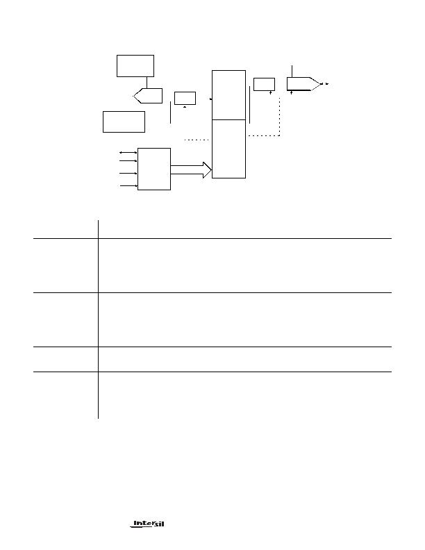
Block Diagram
Pin Description
SDA
SCL
WP
2-WIRE
I
OUT
INTERFACE
A2, A1, A0
DAC
ADC
LOOK-UP
TABLE
CONTROL
AND STATUS
MUX
MUX
TEMPERATURE
SENSOR
VOLTAGE
REFERENCE
PIN
NUMBER
PIN
NAME
DESCRIPTION
1
A0
Device Address Select Pin 0. This pin determines the LSB of the device address
required to communicate using the 2-wire interface. The A0 pin has an on-chip pull-down resistor.
2
A1
Device Address Select Pin 1. This pin determines the intermediate bit of the device address required to communicate
using the 2-wire interface. The A1 pin has an on-chip pull-down resistor.
3
A2
Device Address Select Pin 2. This pin determines the MSB of the device address required to communicate using the
2-wire interface. The A2 pin has an on-chip pull-down resistor.
4
V
CC
Supply Voltage.
5
WP
Write Protect Control Pin. This pin is a CMOS compatible input. When LOW, Write Protection is enabled preventing
any
Write
operation. When HIGH, various areas of the memory can be protected using the Block Lock bits BL1 and
BL0. The WP
pin has an on-chip pull-down resistor, which enables the Write Protection when this pin is left floating.
6
SCL
Serial Clock. This is a TTL compatible input pin. This input is the 2-wire interface clock controlling data input and output
at the SDA pin.
7
SDA
Serial Data. This pin is the 2-wire interface data into or out of the device. It is TTL
compatible when used as an input, and it is Open Drain when used as an output. This pin requires an external pull up
resistor.
8
I
OUT
Current Generator Output. This pin sinks or sources current. The magnitude and direction of the current is fully
programmable and adaptive. The resolution is 8 bits.
9, 10,
12,13,14
NC
No Connect.
11
V
SS
Ground.
X96011
发布紧急采购,3分钟左右您将得到回复。
相关PDF资料
XR4151CP-F
IC CONV VF/FV 8PDIP
XRP7714ILB-0X14-F
IC REG 5OUT BCK/LINEAR 40TQFN
XRP7740ILB-0X18-F
IC REG 5OUT BCK/LINEAR 40TQFN
XRP7740ILBTR-F
IC REG 5OUT BCK/LINEAR 40TQFN
ZDS1009TA
IC CURRENT MIRROR SOT223-8
ZXCT1008FTA
IC CURRENT MONITOR 1% SOT23-3
ZXCT1009T8TA
IC CURRENT MONITOR 1% SM8
ZXCT1010E5TA
IC CURRENT MONITOR 1% SOT-23-5
相关代理商/技术参数
X96012
制造商:INTERSIL 制造商全称:Intersil Corporation 功能描述:Universal Sensor Conditioner with Dual Look-up Table Memory and DACs
X96012_08
制造商:INTERSIL 制造商全称:Intersil Corporation 功能描述:Universal Sensor Conditioner with Dual Look-up Table Memory and DACs
X96012V14I
功能描述:IC CNTRLR UNIV MEM/DAC 14-TSSOP RoHS:否 类别:集成电路 (IC) >> 接口 - 传感器和探测器接口 系列:- 其它有关文件:Automotive Product Guide 产品培训模块:Lead (SnPb) Finish for COTS
Obsolescence Mitigation Program 标准包装:74 系列:- 类型:触控式传感器 输入类型:数字 输出类型:数字 接口:JTAG,串行 电流 - 电源:100µA 安装类型:表面贴装 封装/外壳:20-TSSOP(0.173",4.40mm 宽) 供应商设备封装:20-TSSOP 包装:管件
X96012V14IZ
功能描述:板上安装温度传感器 UNIVERSAL SENSOR CONDITIO W/DL LOOKUP RoHS:否 制造商:Omron Electronics 输出类型:Digital 配置: 准确性:+/- 1.5 C, +/- 3 C 温度阈值: 数字输出 - 总线接口:2-Wire, I2C, SMBus 电源电压-最大:5.5 V 电源电压-最小:4.5 V 最大工作温度:+ 50 C 最小工作温度:0 C 关闭: 安装风格: 封装 / 箱体: 设备功能:Temperature and Humidity Sensor
X96012V14IZT1
功能描述:板上安装温度传感器 UNIVERSAL SENSOR CONDITIO W/DL LOOKUP RoHS:否 制造商:Omron Electronics 输出类型:Digital 配置: 准确性:+/- 1.5 C, +/- 3 C 温度阈值: 数字输出 - 总线接口:2-Wire, I2C, SMBus 电源电压-最大:5.5 V 电源电压-最小:4.5 V 最大工作温度:+ 50 C 最小工作温度:0 C 关闭: 安装风格: 封装 / 箱体: 设备功能:Temperature and Humidity Sensor
X9601XEVAL
制造商:Intersil Corporation 功能描述:X9601 EVALUATION BOARD - Bulk
X9650M
制造商:EPCOS 制造商全称:EPCOS 功能描述:Bandpass Filter
X-97-488
制造商:Brady Corporation 功能描述:Labels External Width:0.9" 制造商:Brady Corporation 功能描述:LABEL IDENTIFICATION 22.86X22.86 BLK/WHT; Background Color:White; Color:Black on White; External Width:0.9"; For Use With:IDXPERT Hand-Held Labeler; Label Material:Polyester; Label Size:22.86 x 22.86mm; Label Type:Identification ;RoHS Compliant: Yes
